Customise Training

TechSource Systems is MathWorks Authorised Reseller and Training Partner

Comprehensive training which provides minimum requirement for FPGA related project readiness.

‘Verilog & FPGA Design’ is a comprehensive training package that comprises of 2 course modules: Designing with Verilog and Designing FPGAs Using the Vivado Design Suite 1. Based on Xilinx industry standard, this 6-day training package can be considered as the minimum training requirement for project readiness.
Designing with Verilog (3-day) is a comprehensive course which provides a thorough introduction to the Verilog language. The emphasis is on writing Register Transfer Level (RTL) and behavioral source code. This class addresses targeting Xilinx devices specifically and FPGA devices in general. The information gained can be applied to any digital design by using a top-down synthesis design approach. This course combines insightful lectures with practical lab exercises to reinforce key concepts. You will also learn advanced coding techniques that will increase your overall Verilog proficiency and enhance your FPGA optimization. This course covers Verilog 1995 and 2001. You will gain valuable hands-on experience. Incoming students with little or no Verilog knowledge will finish this course empowered with the ability to write efficient hardware designs and perform high-level HDL simulations.
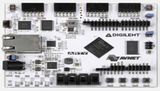
Designing FPGAs Using the Vivado Design Suite 1 (2-day) offers introductory training on the Vivado® Design Suite and demonstrates the FPGA design flow for those uninitiated to FPGA design.
The course provides experience with creating a Vivado Design Suite project with source files, simulating a design, performing pin assignments, applying basic timing constraints, synthesizing and implementing, debugging a design, generating and downloading a bitstream onto a demo board.
Hands-on Project (1-day) on the last day allows you to test your knowledge and apply your skills immediately. No documentation, no labs instructions, you will face the real challenge to do a full FPGA design flow project with the guidance of our instructor.

Digital designers who are interested in FPGA design training and want to use Verilog effectively for modeling, design, and synthesis of digital designs and learn to use Xilinx FPGAs.

Basic digital design knowledge.

After completing this comprehensive training, you will have the
necessary skills to do the following:
Designing with Verilog
FPGA Design Expert
TechSource Systems is MathWorks Authorised Reseller and Training Partner
Objective: Discusses the history of the Verilog language and provides an overview of the different features of Verilog.
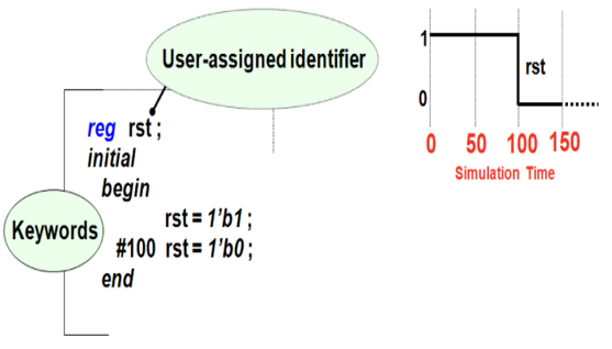
Objective: Discusses the data objects that are available in the Verilog language as well as keywords and identifiers.
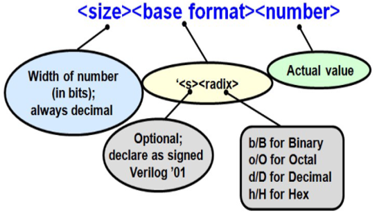
Objective: Covers what data values are in Verilog, as well as how to represent numbers in Verilog.
Objective: Covers the various data types in Verilog.
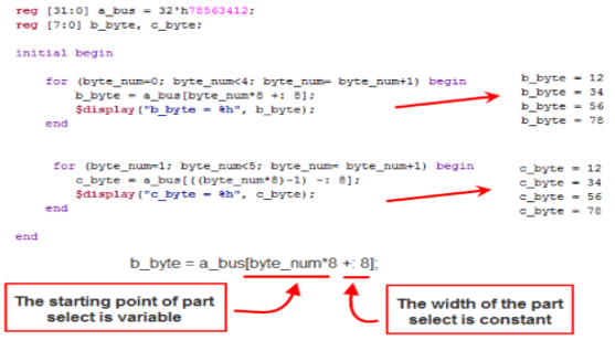
Objective: Covers buses and arrays in Verilog.
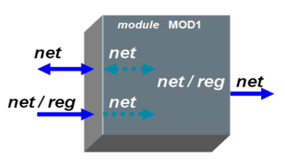
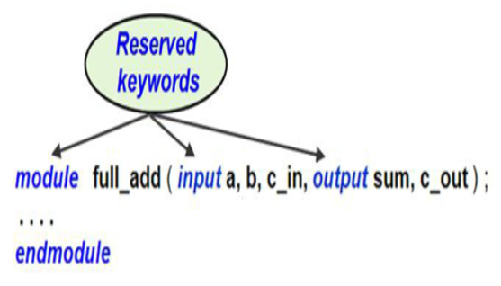
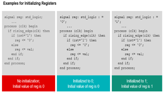
Objective: Describes both the syntax and hierarchy for a Verilog module, port declarations, and the difference between reg versus wire.
Objective: Shows the syntax for all Verilog operators.
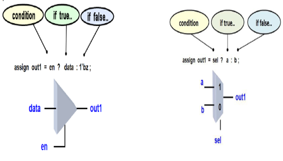
Objective: Introduces the Verilog continuous assignment statement.
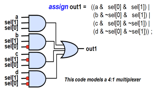
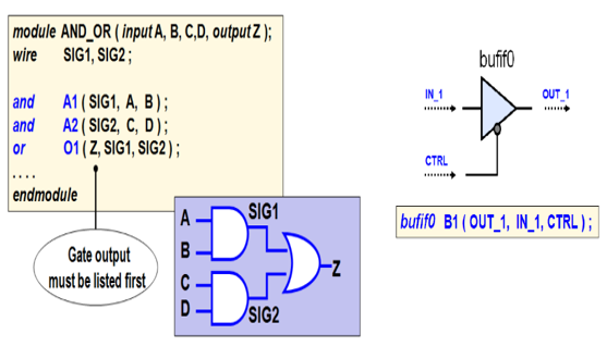
Objective: Introduces gate-level modeling in Verilog.
Objective: Provides an introduction to procedural assignments in Verilog, including their usage and restrictions.
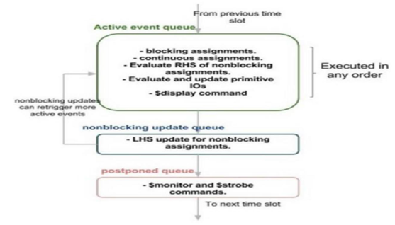
Objective: Introduces blocking and non-blocking assignment statements in Verilog.
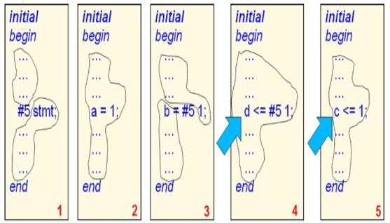
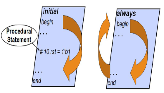
Objective: Introduces the timing control methods that are used in procedural assignments.
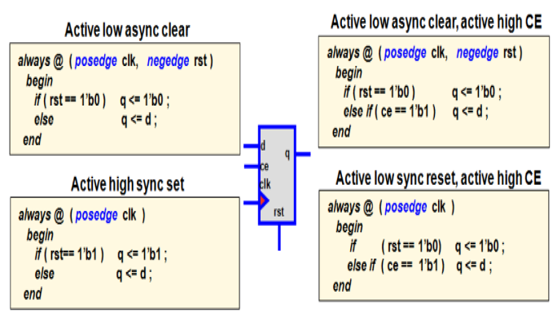
Objective: Describes the if/else conditional statement.
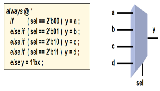
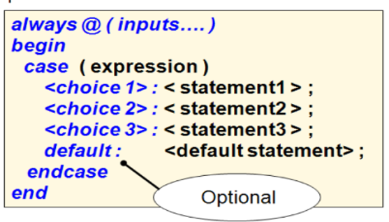
Objective: Describes the case conditional statement.
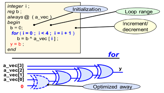
Objective: Introduces the different types of Verilog loop statements.
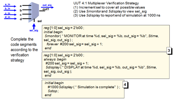
Objective: Introduces the concept of the Verilog testbench.
Objective: Provides a basic understanding of system tasks.
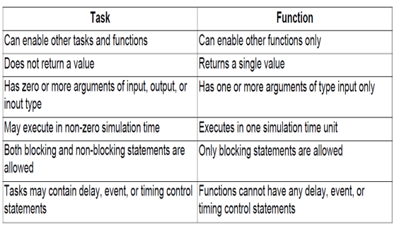
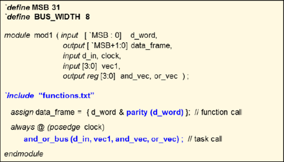
Objective: Covers the use of subprograms in verification and RTL code to model functional blocks.
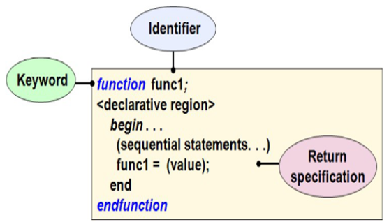
Objective: Describes functions, which are integral to reusable and maintainable code.
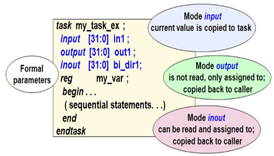
Objective: Covers tasks in Verilog.
Objective: Describes Verilog compiler directives.
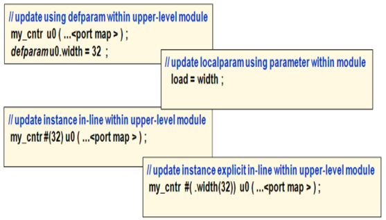
Objective: Covers Verilog parameters and the local parameter concept.
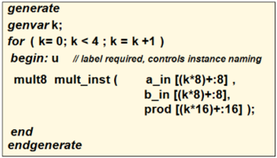
Objective: Introduces the Verilog generate statement.
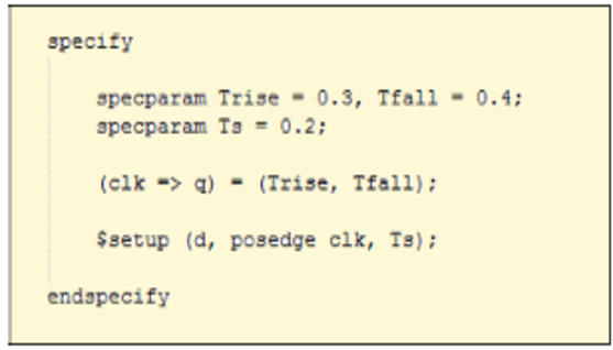
Objective: Covers the timing check statements in Verilog and talks about the specify block.
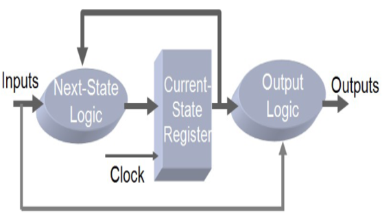
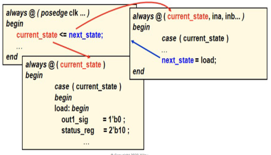
Objective: Provides an overview of finite state machines, one of the more commonly used circuits.
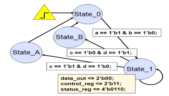
Objective: Describes the Mealy FSM and how to code for it.
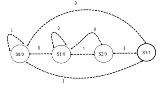
Objective: Describes the Moore FSM and how to code for it.
Objective: Shows how to model an FSM of any complexity in Verilog and describes recommendations for performance and reliability.
Objective: Objective: Describe what a race condition is and provides steps to avoid this condition.
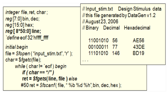
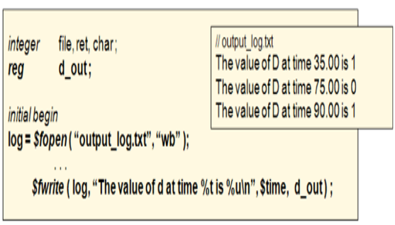
Objective: Covers using basic and enhanced Verilog file I/O capabilities for more robust design verification.
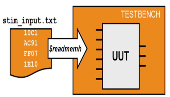
Objective: Objective: Covers Verilog file I/O read capabilities.
Objective: Covers Verilog file I/O write capabilities.
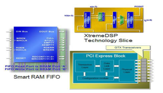
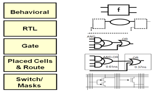
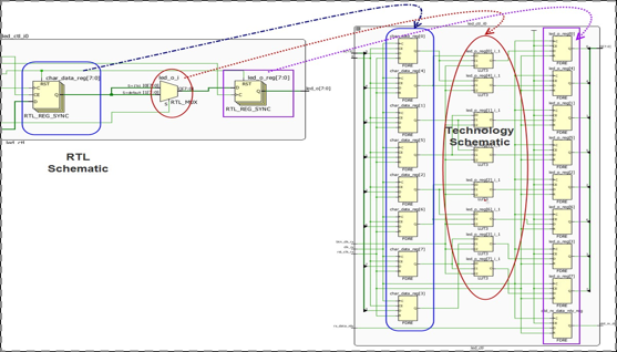
Objective: Focuses on Xilinx-specific implementation and chip-level optimization.
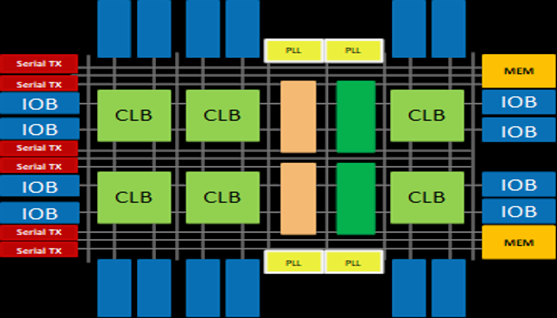
Objective: Overview of FPGA architecture, SSI technology, and SoC device architecture.
Objective: Introduces the methodology guidelines covered in this course and the UltraFast Design Methodology checklist.
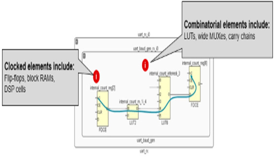
Objective: Covers basic digital coding guidelines used in an FPGA design.
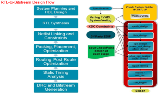
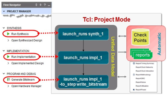
Objective: Introduces the Vivado design flows: the project flow and non-project batch flow.
Objective: Introduces the project-based flow in the Vivado Design Suite: creating a project, adding files to the project, exploring the Vivado IDE, and simulating the design.
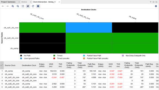
Objective: Generate and use Vivado timing reports to analyze failed timing paths.
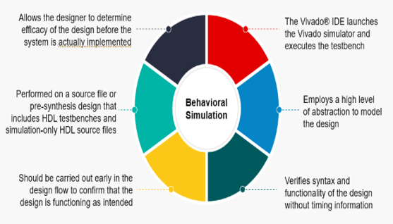
Objective: Describes the process of behavioral simulation and the simulation options available in the Vivado® IDE.
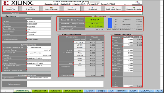
Objective: Estimate the amount of resources and default activity rates for a design and evaluate the estimated power calculated by XPE.
Objective: Create timing constraints according to the design scenario and synthesize and implement the design. Optionally, generate and download the bitstream to the demo board.
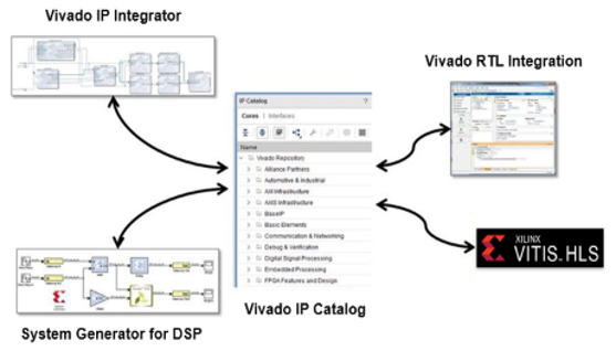
Objective: Customize IP, instantiate IP, and verify the hierarchy of your design IP.
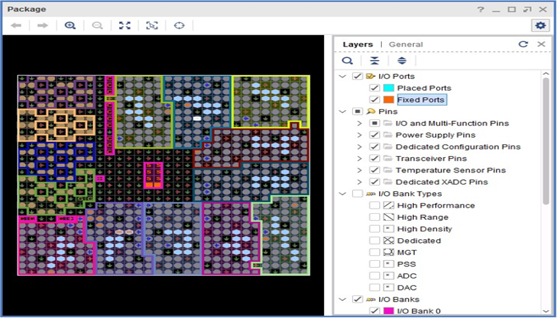
Objective: Use the I/O Pin Planning layout to perform pin assignments in a design.
Objective: Apply clock constraints and perform timing analysis.
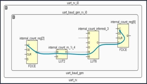
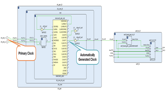
Objective: Use the report clock networks report to determine if there are any generated clocks in a design.
Objective: Apply I/O constraints and perform timing analysis.
Objective: Use the Timing Constraints Wizard to apply missing timing constraints in a design.
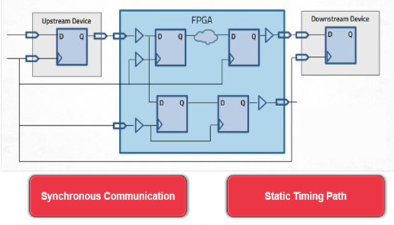
Objective: Describes the basics of clock gating and static timing analysis.
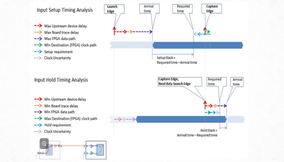
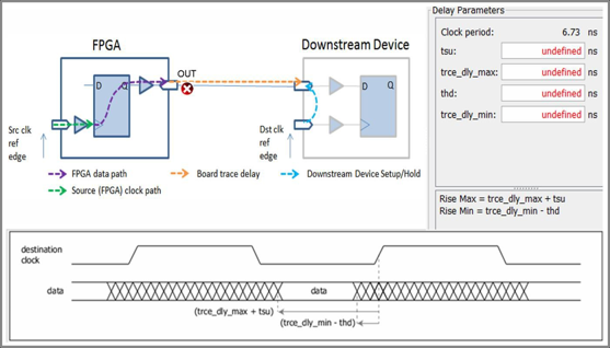
Objective: Reviews setup and hold timing calculations.
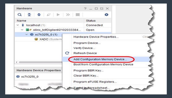
Objective: Describes how FPGAs can be configured.
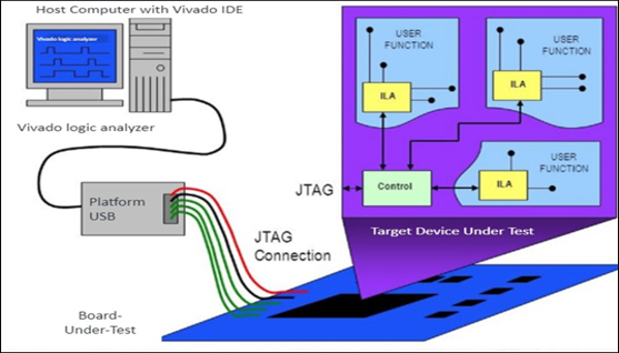
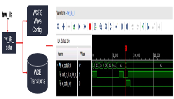
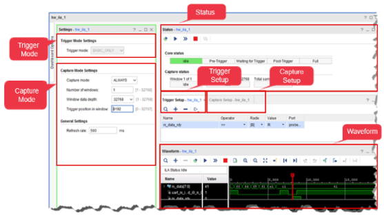
Objective: Overview of the Vivado logic analyzer for debugging a design.
Objective: Introduces the trigger capabilities of the Vivado logic analyzer.
Objective: Understand how the debug hub core is used to connect debug cores in a design.
Objective: Introduces Tcl (tool command language).
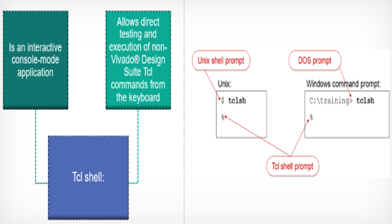
Objective: Understand the Tcl syntax and structure.
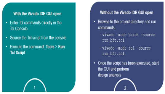
Objective: Explains what Tcl commands are executed in a Vivado Design Suite project flow.
FPGA Design Flow Hands-on practices.