


 Customise Your Training

TechSource Systems is MathWorks Authorised Reseller and Training Partner
Connectivity Design
Learn when and how to apply signal integrity techniques to high-speed interfaces between Xilinx FPGAs and other components.

This three-day comprehensive course combines design techniques and methodology with relevant background concepts of high-speed bus and clock design, including transmission line termination, loading, and jitter.
You will work with IBIS models and complete simulations using Mentor Graphics HyperLynx. Other topics include managing PCB effects and on-chip termination. This course balances lecture modules with instructor demonstrations and practical hands-on labs.

Digital designers, board layout designers, or scientists, engineers, and technologists seeking to implement Xilinx solutions. Also end users of Xilinx products who want to understand how to implement high-speed interfaces without incurring the signal integrity problems related to timing, crosstalk, and overshoot or undershoot infractions.


After completing this comprehensive training, you will have the
necessary skills to:
TechSource Systems is MathWorks Authorised Reseller and Training Partner
Objective: introduce the Signal Integrity part of the course. Describe transmission lines. Interpret an IBIS model and correct common errors. Work with a signal integrity tool. Apply appropriate transmission line termination. Simulate simple trace structures. Simulate more complex structures like serial I/O or memory interfaces. Evaluate a design for the potential of signal degradation from signal propagation, reflection, crosstalk, and power supply. Recognize and mitigate the effects of signal propagation, reflection, crosstalk, and power supply on signal integrity.
Objective: Describe the nature of a transmission line. Explain the significance of harmonic magnitude. Discuss the importance of rise and fall times. Identify general issues relating to signal integrity design.
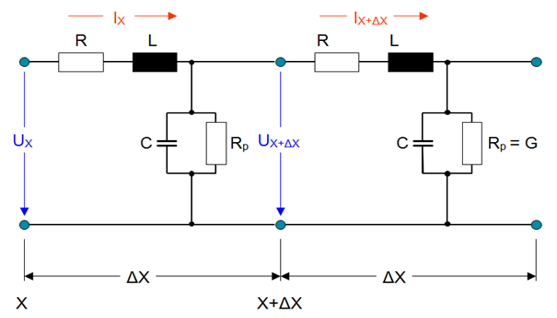
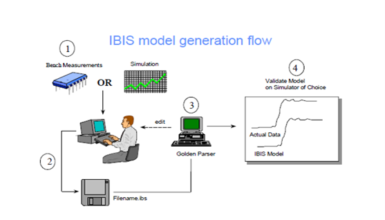
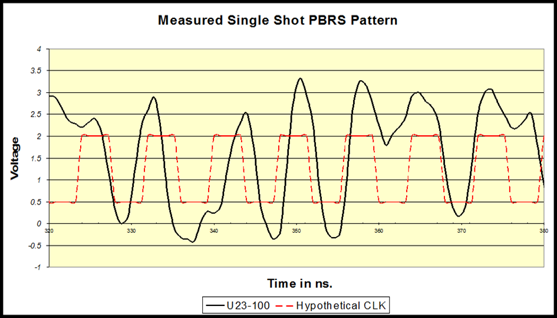
Objective: Describe some modeling and simulation considerations before the discussion on reflection and crosstalk should begin. Describe the IBIS file. Explain the importance of an IBIS editor. Identify the components of an IBIS file. Describe main features of a signal integrity tool. Create simple structures for signal integrity simulation with the HyperLynx tool.
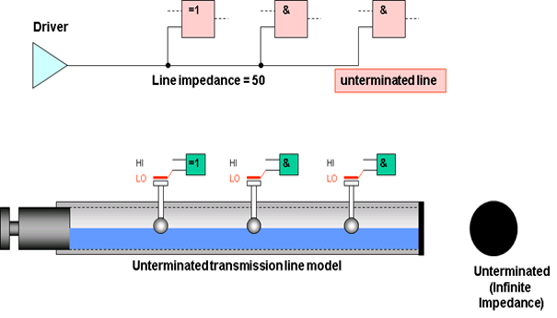
Objective: Discuss reflections on transmission lines. Explain the reflection effect and how to minimize reflection during termination. Describe the effect of reflection. Reduce the reflection by termination. Describe the reflection for different topologies. Simulate reflection effects.
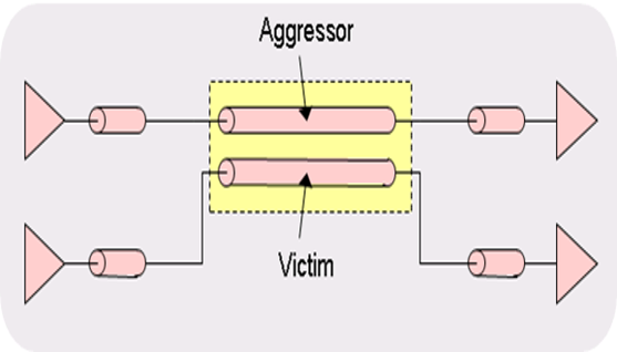
Objective: Describe crosstalk on transmission lines. Explain the crosstalk effect and how to minimize crosstalk by trace geometry or dielectric thickness.
Objective: Describe the principle SI analysis methods. Expand your modeling for packages and vias. Describe system-wide SI analysis. Integrate design kits into your environment.
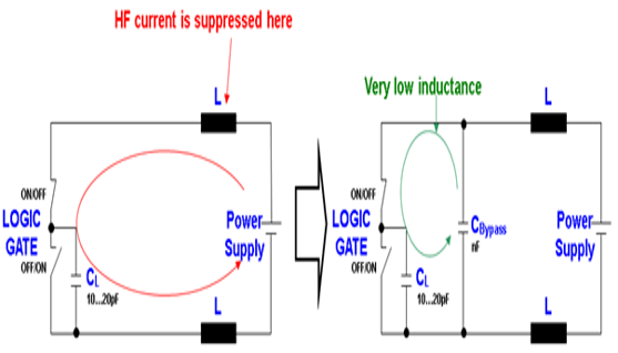
Objective: Describe power supply impedance considerations. Describe power supply inductance considerations. Describe the bypassing capacitor function and realization. Handle SI issues for power supply at the board level.
Objective: Provide a summary of the signal integrity part of the course.
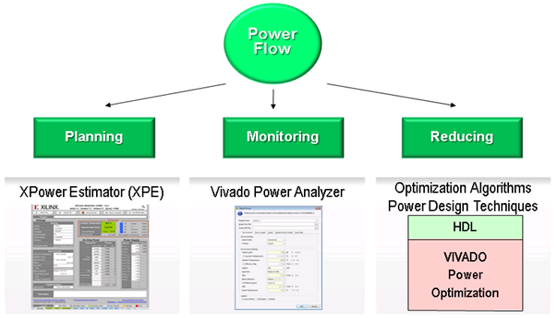
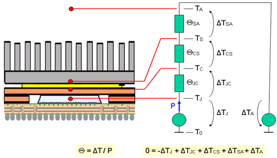
Objective: Determine the power supply requirements for a PCB. Realize an appropriate power supply on a PCB. Realize configuration solutions on a PCB. Describe the requirements and realizations for signal interfacing. Describe some PCB considerations. Evaluate FPGA thermal aspects for a PCB and design appropriate thermal management. Identify the tools to apply to particular board design issues.
Objective: Describe power supply impedance considerations. Describe power supply inductance considerations. Describe the bypassing capacitor function and realization. Handle SI issues for power supply at the board level.
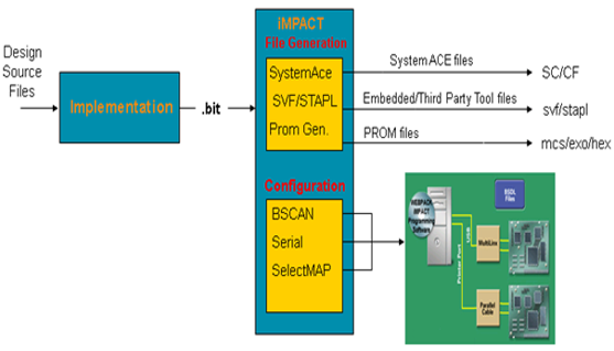
Objective: Describe configuration issues that are important in the board design process. Describe the configuration interfaces and their PCB requirements. Describe the configuration memory and their PCB requirements. Identify some typical configuration applications.
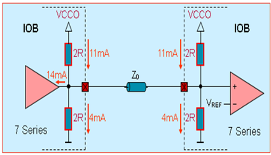
Objective: Describe FPGA interface options and restrictions for clock and data signals. Identify FPGA interfacing resources. Utilize the I/O resources in your design. Describe the combining of different I/O standards. Identify FPGA clocking resources. Apply the physical clocking restriction to your application.
Objective: Describe typical FPGA I/O special standards. Use FPGA interface resources for board design.
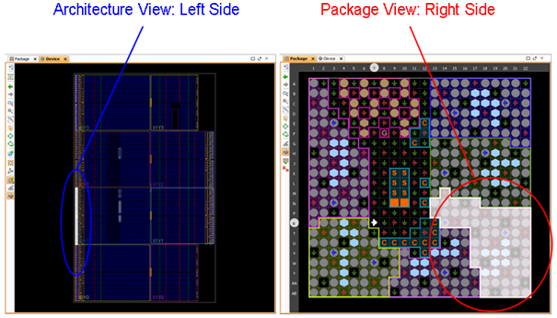
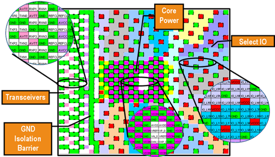
Objective: Use the relationship between chip pad locations and package pin locations for optimal placement of external components. Identify the user pin naming conventions. Evaluate board pin placement for achieving optimum performance.
Objective: Review basic information about the materials and processes for PCBs. Describe how to apply the requirements for signal integrity as well as board design to the realization of the PCB through proper application of the various options for layer stackup. Describe PCB technology. Identify some PCB trace characteristics. Describe aspects of FPGA routability.
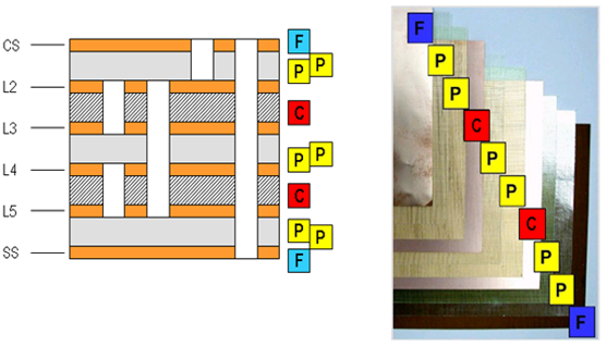
Objective: Review basic information about the materials and processes for PCBs. Describe how to apply the requirements for signal integrity as well as board design to the realization of the PCB through proper application of the various options for layer stackup. Describe PCB technology. Identify some PCB trace characteristics. Describe aspects of FPGA routability.
Objective: Summarize helpful tools for the board design planning process such as power estimation, simulation of transmission lines, power design, simultaneously switching output (SSO), serial backplane transmission, thermal simulation.
Objective: Provide a summary of the board design part of the course such as Layers, Bypassing, Simultaneously switching output (SSO), Signal paths, Power supply and management, Design for debug.